|
Size: 2109
Comment:
|
Size: 2551
Comment:
|
| Deletions are marked like this. | Additions are marked like this. |
| Line 23: | Line 23: |
= Condensed Board = For implementation in tighter spaces, I plan to design a stripped-down board omitting CON1, lines for M1-3 and UC on CON3 and the associated R15-18, using an 8-pin array (Digikey part MSP10KH-ND) for R8-14 and reordering the remaining lines on CON3 to support more direct paths through the PCB, and dropping the GND line from CON4 (since CON3 exposes one anyway). I may also go with lower-profile parts for C4 and X1. |
Contents
Printed Circuit Board Layout
I used Fritzing to lay out a two-layer SpiffChorder development board and submitted an order for the prototype to Fritzing Fab. The fabrication cost for one unit, including international shipping to the USA, was roughly US$40. I'll post pictures once it arrives in a couple weeks and I have a chance to run tests, but here are some preliminary details:
Fritzing's schematic view (printed to PDF at 450x315mm with no margins)
an etchable PDF export from Fritzing (combined using pdfunite from poppler-utils)
a ZIP archive of the Gerber export files for the prototype (sent to me by Fritzing Fab)
Bill of Materials
So far I'm using the same BoM from the perfboard design, but I'll probably switch up CON1 with Digikey part 609-2845-ND (vertical rather than right-angle) so as not to block the lower-left mounting hole.
Paper Placement Test
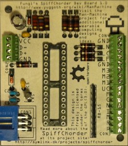
Here's a paper test using a 1:1 scale printout of the silkscreen and solder mask together:
Connector Detail
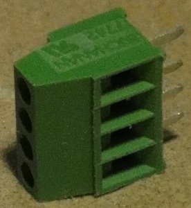
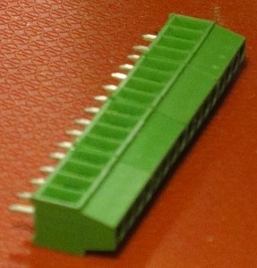
The 0.1" pitch right-angle screw terminal blocks I used are just slightly longer than 0.4" each. So as to be able to fit the four for CON3-4 directly adjacent to one another, I lightly sanded the facing sides until they fit snugly but evenly in a piece of perfboard. In an effort to make it easier to solder these evenly on the board, I attached their sides together with a tiny dab of quick-setting adhesive gel (being careful not to get it into the terminals themselves):


Condensed Board
For implementation in tighter spaces, I plan to design a stripped-down board omitting CON1, lines for M1-3 and UC on CON3 and the associated R15-18, using an 8-pin array (Digikey part MSP10KH-ND) for R8-14 and reordering the remaining lines on CON3 to support more direct paths through the PCB, and dropping the GND line from CON4 (since CON3 exposes one anyway). I may also go with lower-profile parts for C4 and X1.

 To the extent possible under law, the creator of this work has waived all copyright and related or neighboring rights to it.